ddr4 pcb layout guidelines Ddr pcb layout guidelines Pcb design rules and tips
If you are looking for PCB Routing Guidelines for DDR4 Memory Devices and Impedance | Blog you've visit to the right page. We have 25 Pictures about PCB Routing Guidelines for DDR4 Memory Devices and Impedance | Blog like Ddr Pcb Layout Guidelines, Ddr Pcb Layout Guidelines and also Navigate DDR3 PCBs: The Guide for Understanding. Here you go:
PCB Routing Guidelines For DDR4 Memory Devices And Impedance | Blog
 resources.altium.com
Introduction To Intel's PCB Tabbed Routing Technology
 www.tf-pcb.com
Ddr Pcb Layout Guidelines
 lessonlibrarypanaches.z13.web.core.windows.net
Ddr4 Pcb Layout Guidelines - Uppress
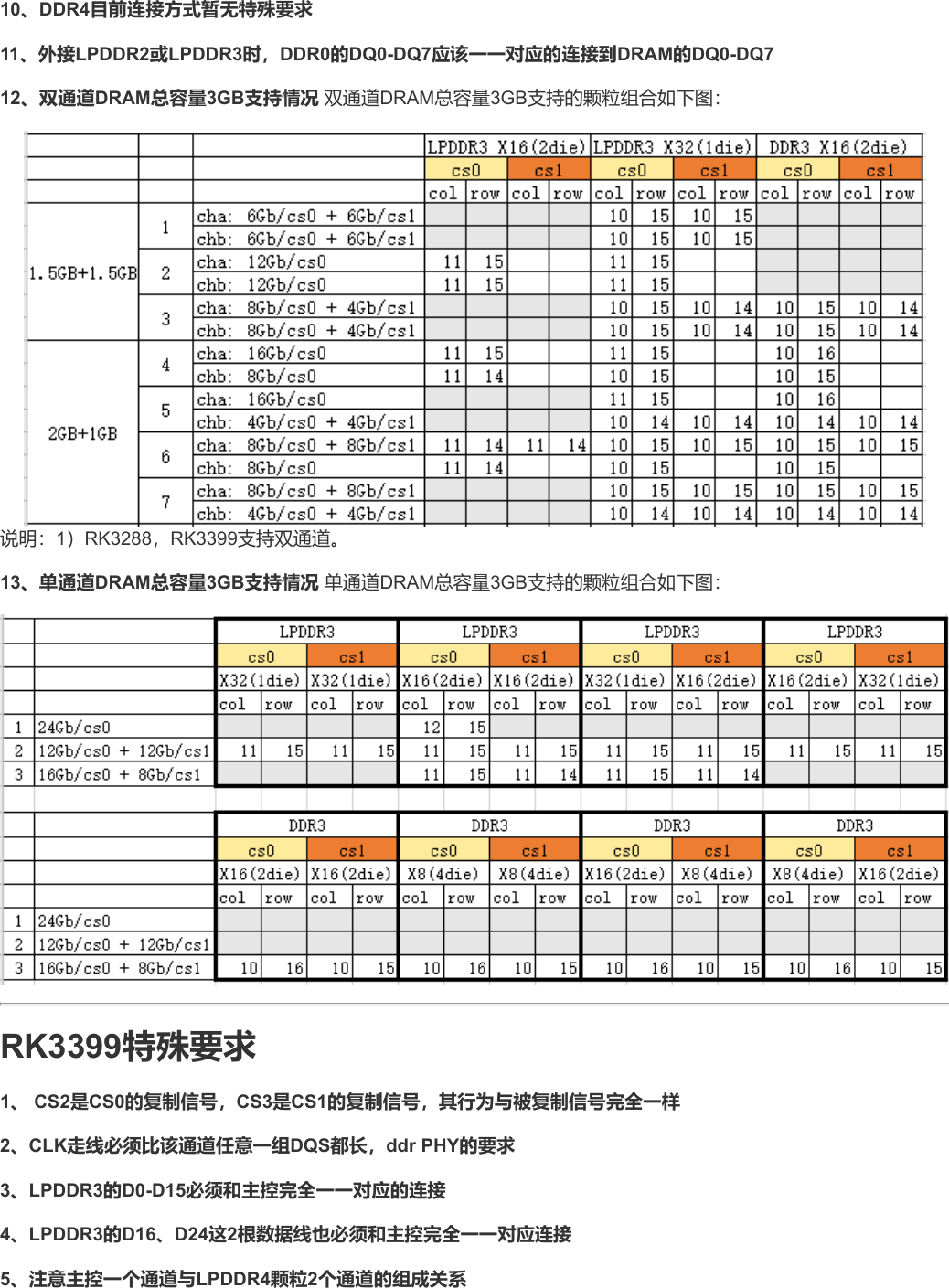
 uppress4.blogspot.com
Section II. PCB Layout Guidelines
 www.yumpu.com
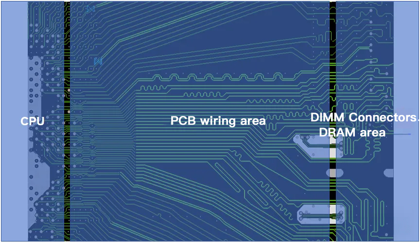
How To Plan For DDR Routing In PCB Layout
 resources.pcb.cadence.com
routing ddr pcb design layout plan memory successful setting
DDR4 PCB Layout: Best Practices For Optimal Performance – Hillman
 hillmancurtis.com
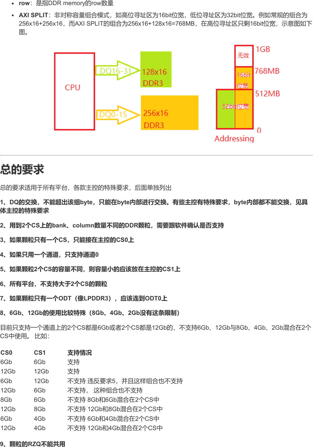
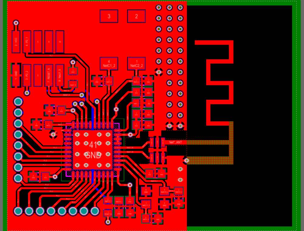
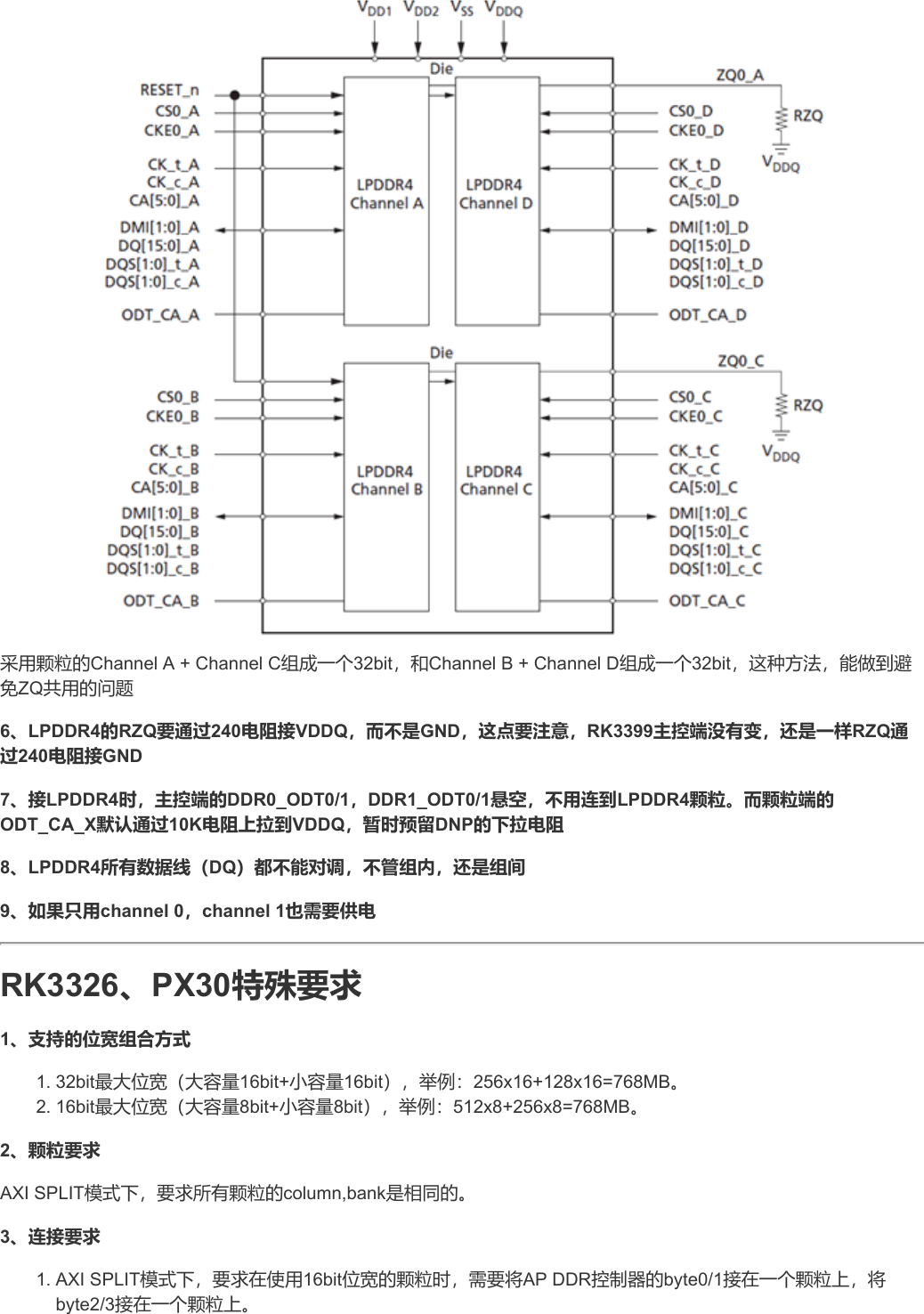
Rockchip Guide DDR PCB Layout Notes CN
 usermanual.wiki
Rockchip Guide DDR PCB Layout Notes CN
 usermanual.wiki
Ddr Pcb Layout Guidelines
 studyzoneoverrating.z14.web.core.windows.net
Pcb Design Guidelines Mechanical Layer Eurocircuits Eurocircuits Images
 www.tpsearchtool.com
PCB Routing Guidelines For DDR4 Memory Devices And Impedance | Blog
 resources.altium.com
ddr4 topology routing guidelines pcb
Ddr3 Layout Guidelines - Diysens
 diysens.blogspot.com
Review Of Server PCB Layout & Schematic – Part 6: DDR4 Memory Layout
 www.learnpcb.com
layout schematic pcb ddr4
High Speed Pcb Layout Guidelines - Design Talk
 design.udlvirtual.edu.pe
PCB Design Rules And Tips
 www.6pcb.com
DDR4 PCB Layout: Best Practices For Optimal Performance – Hillman
 hillmancurtis.com
A1 A2 Sodimm Ddr4 Pcb Layout Guidelines Ddr3 Ram Pcb Design 2.0mm From
 mart.ecer.com
Ddr Pcb Layout Guidelines
 learningschoolunavowed.z14.web.core.windows.net
A1 A2 Sodimm Ddr4 Pcb Layout Guidelines Ddr3 Ram Pcb Design 2.0mm From
 mart.ecer.com
Navigate DDR3 PCBs: The Guide For Understanding
 www.venture-mfg.com
Rockchip Guide DDR PCB Layout Notes CN
 usermanual.wiki
High Speed Printed Circuit Board (PCB) Design Guidelines – PCB HERO
 www.pcb-hero.com
DDR, DDR2 And DDR3 – PCB Layout Examples
 www.fedevel.com
PCB Routing Guidelines For DDR4 Memory Devices And Impedance | Blog
 resources.altium.com
ddr4 termination pcb routing guidelines clk altium
A1 a2 sodimm ddr4 pcb layout guidelines ddr3 ram pcb design 2.0mm from. High speed printed circuit board (pcb) design guidelines – pcb hero. Rockchip guide ddr pcb layout notes cn