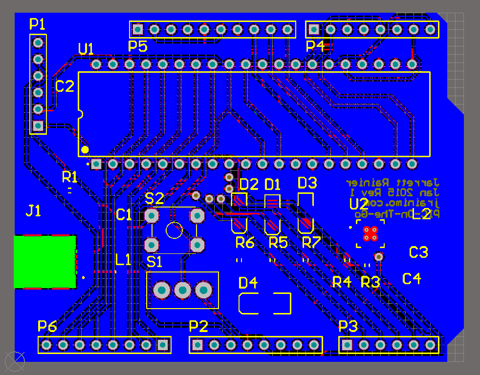
Desain Layout PCB by EDY Tips and tricks to follow for a quality pcb layout : part 1 Dc/dc converter pcb layout, part 1
If you are searching about High-Quality PCB Layout and Assembly Solution - China PCB Design and you've visit to the right place. We have 25 Pics about High-Quality PCB Layout and Assembly Solution - China PCB Design and like Tips and Tricks for an Efficient PCB Layout - Blog PCB Unlimited, Altium designer pcb layout part 1 - copysop and also Jual Jasa Desain Layout PCB Segala Rangkaian | Shopee Indonesia. Here you go:
High-Quality PCB Layout And Assembly Solution - China PCB Design And
 zinponpcb.en.made-in-china.com
Schematic Diagram To Pcb Layout Converter
 www.circuitdiagram.co
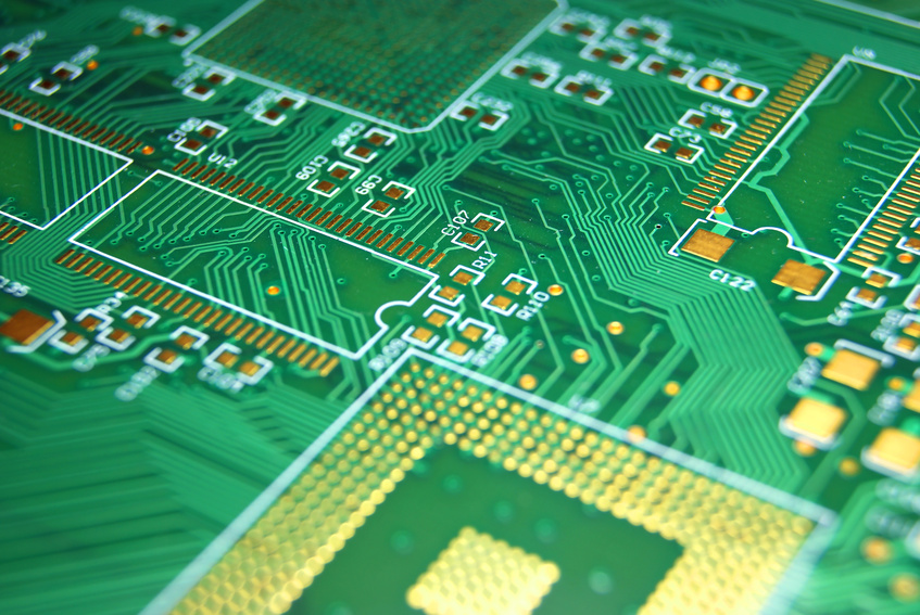
18 PCB Layout Tips For Improving Your PCB Design And Reducing
 camptechii.com
pcb design layout trace tips spacing traces manufacturing headaches board copper side out ground between pads using each opposite improving
Altium Designer Pcb Layout Part 1 - Seeklke
 seeklke.weebly.com
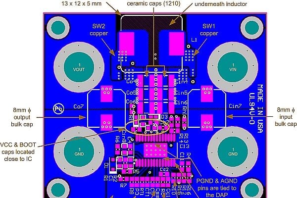
DC/DC Converter PCB Layout, Part 1 - EDN
 www.edn.com
pcb converter layout edn
Altium Designer Pcb Layout Part 1 - Copysop
 copysop.weebly.com
High Quality PCB Layout And Design Services Available - China Quality
 zinponpcb.en.made-in-china.com
Altium Designer Pcb Layout Part 1 - Lasopatemplates
 lasopatemplates218.weebly.com
Tips And Tricks For An Efficient PCB Layout - Blog PCB Unlimited
 www.pcbunlimited.com
pcb layout blog tips
Altium Designer Pcb Layout Part 1 - Copysop
 copysop.weebly.com
Jual Jasa Desain Layout PCB Segala Rangkaian | Shopee Indonesia
High-Quality PCB Layout And Assembly Service - China High-Quality PCB
 zinponpcb.en.made-in-china.com
PCB Layout Optimization For EMI And EMC
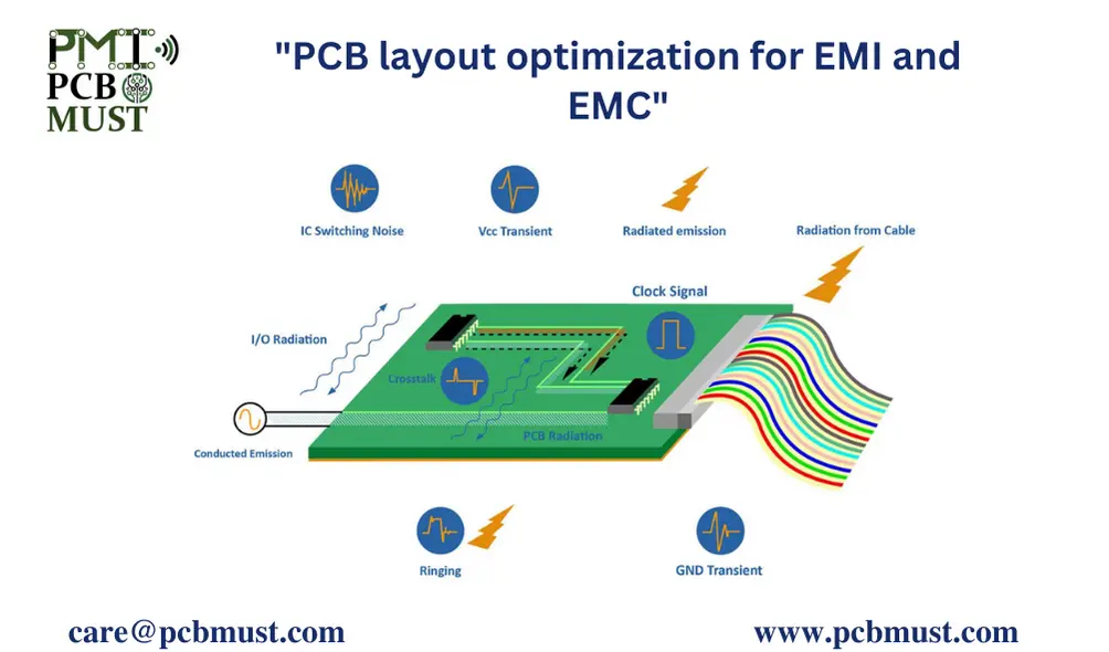 pcbmust.com
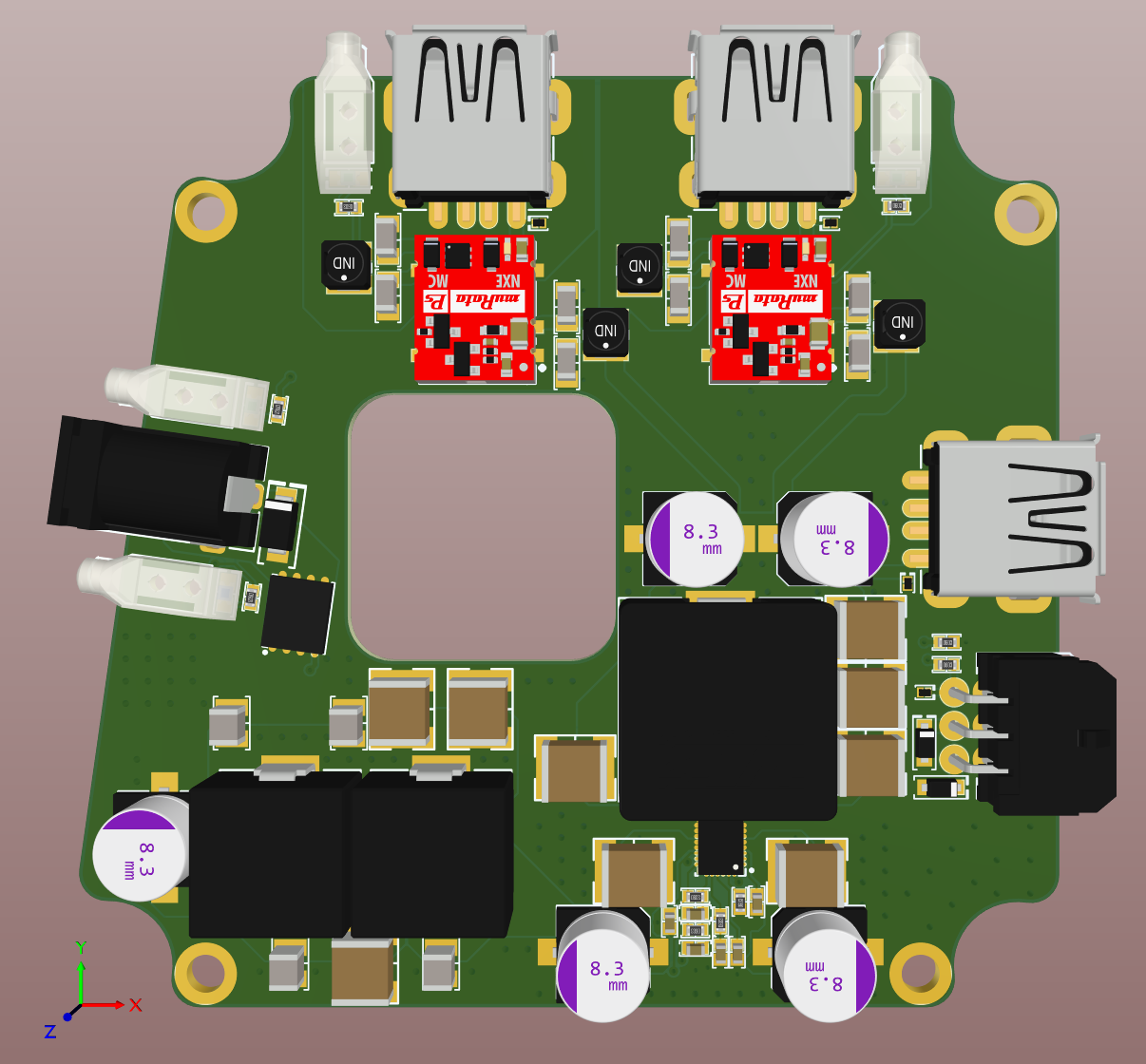
DC/DC Converter PCB Layout, Part 3
 www.eenewseurope.com
Do Professional Quality Pcb Layout In Kicad By Such__
 www.fiverr.com
kicad pcb layout professional quality do screen full
Altium Designer Pcb Layout Altium Designer Pcb Layout
 pcbways.pages.dev
DC/DC Converter PCB Layout, Part 1
 www.eenewspower.com
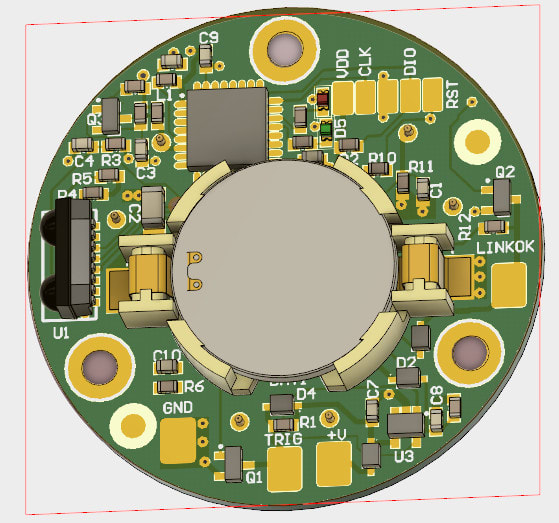
PCB Layout Tutorial
 mungfali.com
High-Quality PCB Layout And Manufacturing - China PCB Layout And
 zinponpcb.en.made-in-china.com
Schematic Diagram To Pcb Layout Converter
 www.circuitdiagram.co
Altium Designer Pcb Layout Part 1 - Jawermiles
 jawermiles.weebly.com
DC/DC Converter PCB Layout, Part 2
 www.eenewspower.com
DC/DC Converter PCB Layout, Part 1 - EDN
 www.edn.com
converter pcb edn
DC/DC Converter PCB Layout, Part 1 - EDN
 www.edn.com
edn converter pcb
DC/DC Converter PCB Layout, Part 1 - EDN
 www.edn.com
pcb converter edn pairs
Pcb design layout trace tips spacing traces manufacturing headaches board copper side out ground between pads using each opposite improving. Dc/dc converter pcb layout, part 1. Dc/dc converter pcb layout, part 3