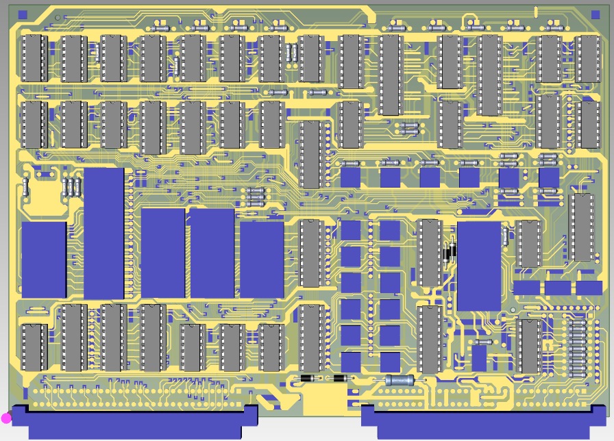
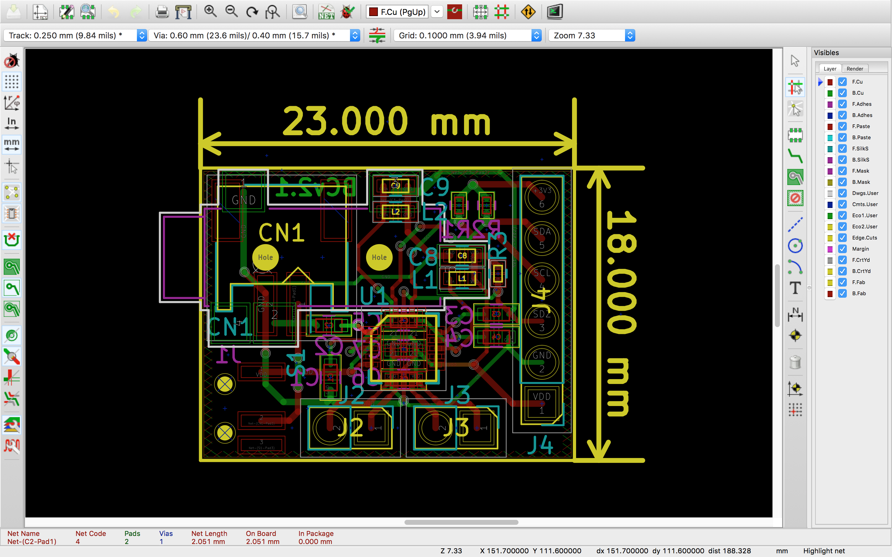
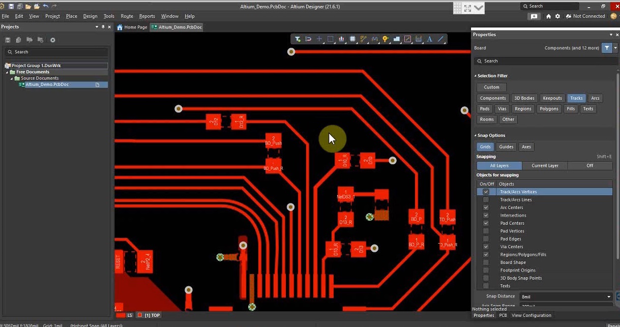
kumpulan skema layout pcb How to do a pcb layout review How to perform pcb design review and layout clean-up
If you are searching about PCB Layout - P5 Electronics you've came to the right page. We have 25 Images about PCB Layout - P5 Electronics like PCB Layout | PDF, PCB layout review/advice - General Discussion - Arduino Forum and also PCB Layout Tutorial. Here it is:
PCB Layout - P5 Electronics
 p5electronics.com
How To Do A PCB Layout Review - Fully Charged - Archives - TI E2E
 e2e.ti.com
Pcb Layout - EasyEDA Open Source Hardware Lab
 oshwlab.com
Pcb Layout | Model Scenery Tutorials
 steamtraininfo.com
Pcb Design Review Checklist Power Pcb Layout Guidelines
 pcbways.pages.dev
Pcb_layout - EasyEDA Open Source Hardware Lab
 oshwlab.com
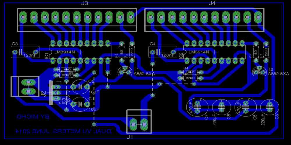
Diagram Skema Dan Lay-Out PCB | PDF
 id.scribd.com
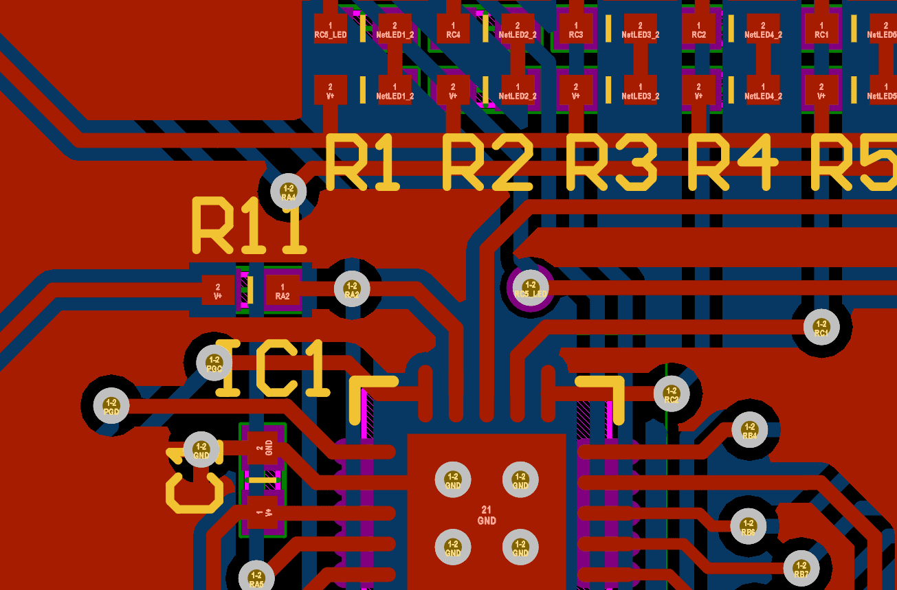
PCB Layout Review/advice - General Discussion - Arduino Forum
 forum.arduino.cc
Your PCB Layout Review Checklist Before Manufacturing | NWES Blog
 www.nwengineeringllc.com
pcb pairs length differential spacing addition checked routing
Guide To PCB Layout Design
 hillmancurtis.com
Your PCB Layout Review Checklist Before Manufacturing | NWES Blog
 www.nwengineeringllc.com
checklist pcb bridging clearance cause polygon solder pads paste
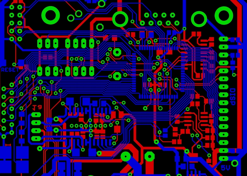
My Progress Of PCB Layout - KENTARO TANAKA
 kentarotanaka.com
schematic pcb progress layout however because did had also work not
Pcb Layout - OSHWLab
 oshwlab.com
PCB Layout Design | TIPSPL
 www.tipspl.com
Complete Guide To PCB Layout Design: Tips, Basics, & Guidelines
 sfxpcb.com
4 Steps To Review The PCB Layout – TechnieX
 techniex.com
Pcb Layout Vs Schematic Drawing » Wiring Diagram
 www.organised-sound.com
Review Of A PCB Layout: Do You Do Same Mistakes? (Part 2 Of 4)
 www.fedevel.com
Terpopuler Layout Pcb Power Gb, Skema Pcb
 skemaelectronikaa.blogspot.com
PCB Layout | PDF
 www.scribd.com
My Progress Of PCB Layout - KENTARO TANAKA
 kentarotanaka.com
pcb placing minimize components both could side
PCB Layout – E-slate
 eslatetech.com
PCB Design Review - Flux - Documentation
 docs.flux.ai
How To Perform PCB Design Review And Layout Clean-Up | Leadsintec
 leadsintec.com
PCB Layout Tutorial
 mungfali.com
Checklist pcb bridging clearance cause polygon solder pads paste. Complete guide to pcb layout design: tips, basics, & guidelines. Pcb_layout